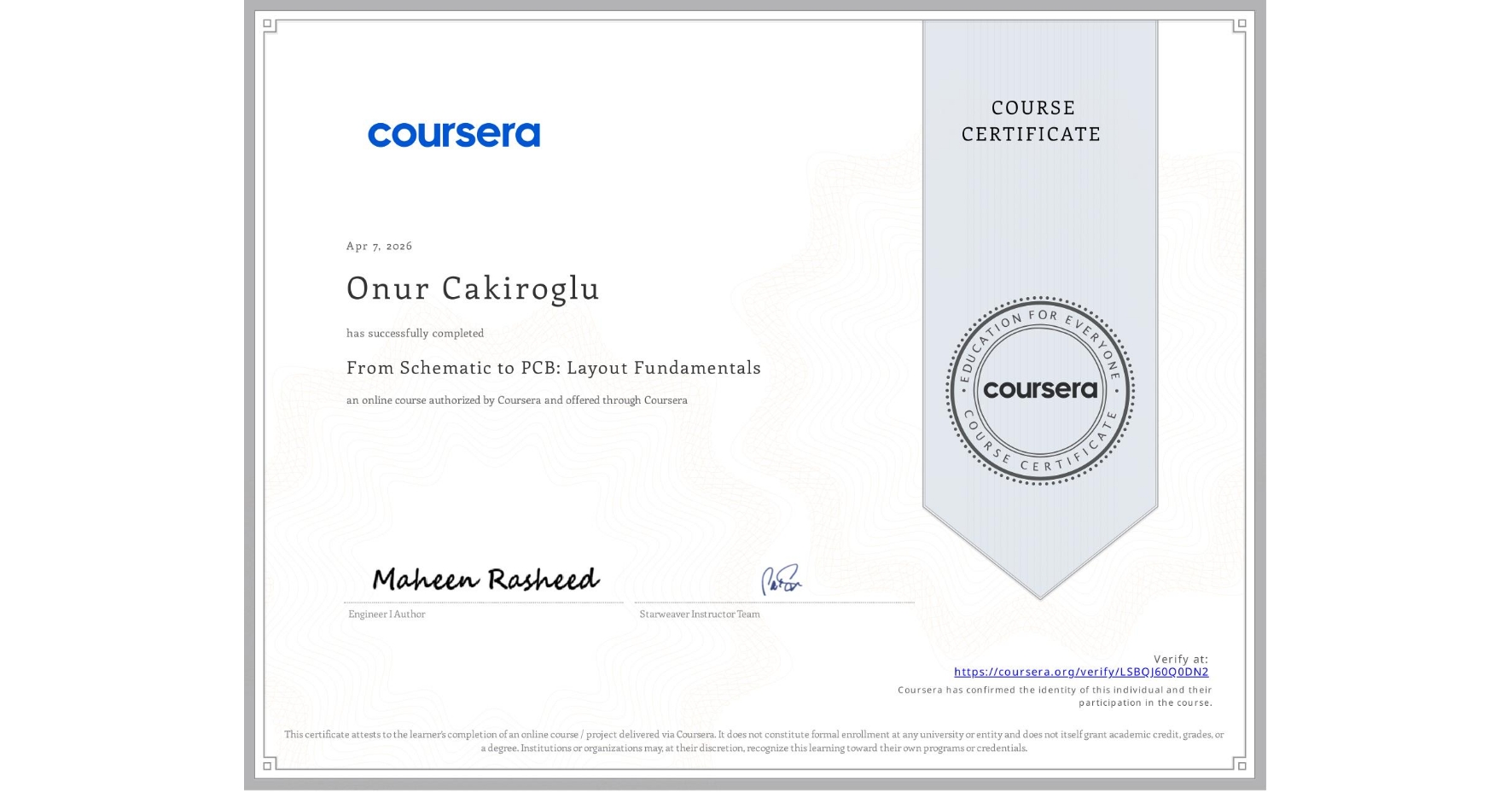
From Schematic to PCB: Layout Fundamentals
Completed by Onur Cakiroglu
April 7, 2026
3 hours (approximately)
Onur Cakiroglu's account is verified. Coursera certifies their successful completion of From Schematic to PCB: Layout Fundamentals

What you will learn
Apply the PCB workflow from schematic to fabrication while applying design rules for trace widths, clearances, and vias.
Implement effective component placement considering signal flow and thermal needs, and design robust power/ground networks.
Integrate power, signals, and high-speed USB differential pairs ensuring signal integrity, and verify designs with ERC/DRC.
Skills you will gain
- Category: Design Specifications
- Category: Design
- Category: Drafting and Engineering Design
- Category: Electronics Engineering
- Category: Electronic Hardware
- Category: Design Strategies
- Category: Electrical Power
- Category: Hardware Design
- Category: Data Import/Export
- Category: Electronics
- Category: Electronic Components
- Category: USB