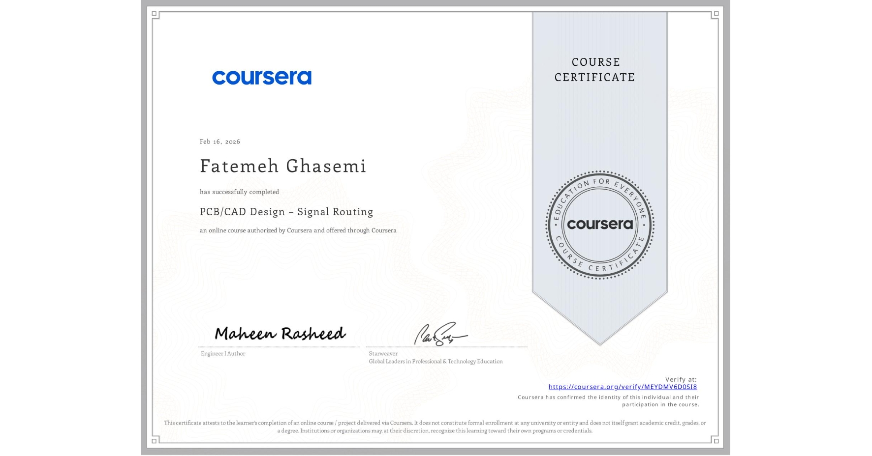
PCB/CAD Design – Signal Routing
Completed by Fatemeh Ghasemi
February 16, 2026
3 hours (approximately)
Fatemeh Ghasemi's account is verified. Coursera certifies their successful completion of PCB/CAD Design – Signal Routing

What you will learn
Explain signal routing & integrity in multilayer PCBs, and describe power/ground design with decoupling & plane management.
Apply controlled impedance and differential pair routing, minimizing crosstalk, reflections, and EMI in high-speed PCB design.
Implement power/ground networks with decoupling and differential pair trace matching, verify designs with DRC/ERC, and generate Gerbers.
Skills you will gain
- Category: Electronics
- Category: Hardware Design
- Category: Electronic Components
- Category: Electronic Hardware
- Category: Schematic Diagrams
- Category: Threat Modeling
- Category: Digital Communications
- Category: Business Strategies
- Category: Model Deployment
- Category: AI Security
- Category: USB
- Category: Electronic Systems