VS
4.0Reviewed May 15, 2026
lecture are a bit short and readings are very long
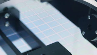
Optical and X-ray techniques are powerful ways to characterize semiconductor thin films. They can be used to measure film thickness, purity and crystalline quality, and for compositional analysis. Modern techniques are fast, turn-key, and generally non-destructive, allowing for rapid assessment of material properties. This course describes the fundamentals of optical and X-ray characterization and provides real-world examples of how they are used in semiconductor manufacturing.
VS
lecture are a bit short and readings are very long
KN
Quick introduction and review of important topics. I wish if more such courses are introduced.
Showing: 8 of 8
Quick introduction and review of important topics. I wish if more such courses are introduced.
Excellent course; I have learned a lot, thanks
Very practical and useful, thanks!
Enjoyed the courses very much!
best course
lecture are a bit short and readings are very long
v.good
I do semiconductor and materials characterization for a living. so this course was too basic in my opinion, its an ok introduction to some of the instruments. Would be nice if there was more exercises like the one used for the solar cell roughness project.